
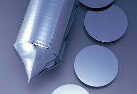

Silicon Wafers
Virginia Semiconductor carries both Single Side Polished (SSP) and Double Side Polished (DSP) wafers available in stock. These wafers range from one to six inches in diameter with other specifications available.

Silicon Ingots
In addition to the common products and sizes, we can make any silicon wafer to any specification, including small, complicated orders. This includes crystal growth, grinding, slicing, lapping, polishing, oxidation, and SOl.

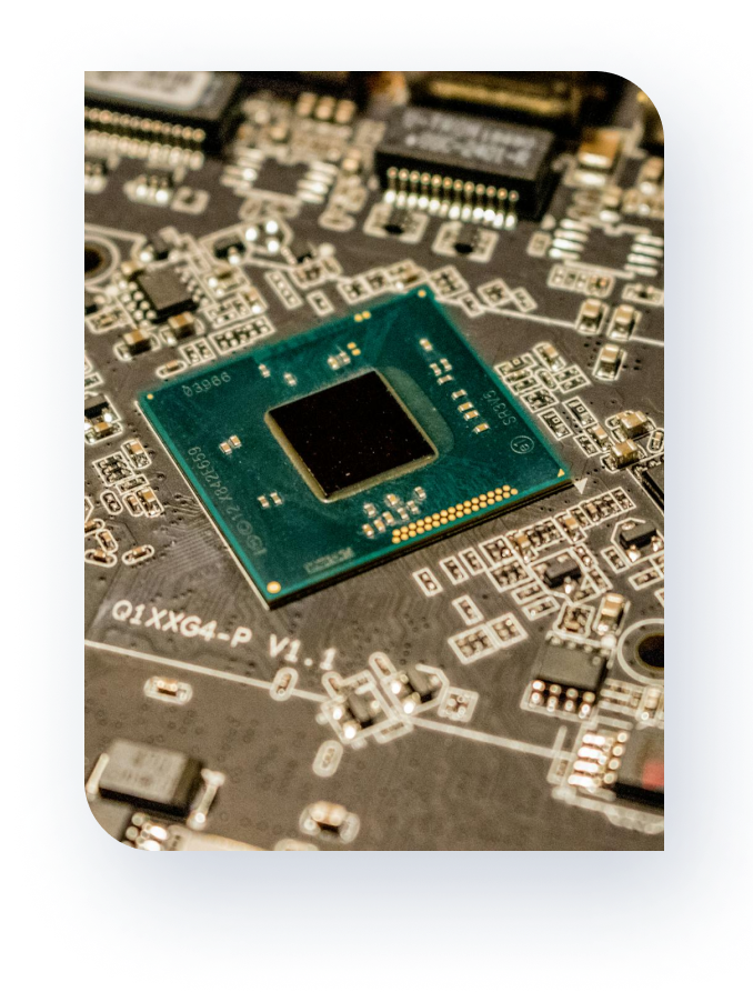
Integrated Circuits
We are a leading manufacturer of prime silicon substrates, offering production quantities of 1-150mm diameter silicon and small quantities of custom silicon substrates. We also offer SOl substrates that range from 25.4mm to 150mm.